學系成員

李清庭 講座教授

  • 學歷

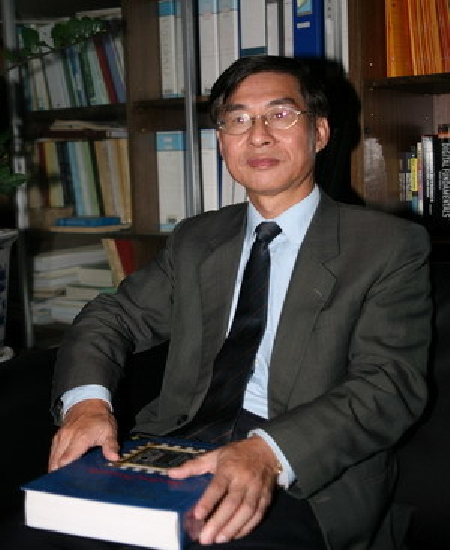
    Carnegie-Mellon University電機研究所博士

    經歷

    • 元智大學光電系教授
    • 國立成功大學名譽講座教授
    • 國立成功大學講座教授
    • 國立成功大學特聘教授
    • 國科會工程處處長
    • 國立成功大學電機資訊學院院長
    • 國立中央大學光電科學研究所教授
    • 中山科學研究院第三研究所技監
    • 中山科學研究院第三研究所副研究員
    • 中山科學研究院第三研究所助理研究員

    研究專長

    研究專長

    積體光學元件及系統/微波半導體工程與元件/光電半導體積體電路

  • 期刊論文

    1. J. W. Wu, C. Y. Chang, K. C. Lin, E. Y. Chang, J. S. Chen and C. T. Lee, "The Thermal Stability of Ohmic Contact to n-type InGaAs Layer", J. Electron. Mater., vol. 24, pp.79-82 (1995)
    2. C. T. Lee, H. P. Shiao and Y. C. Chou, "MESFET Performance and Limitations of Optimized GaAs Strained Buffer Layer Grown on InP by Molecular Beam Epitaxy", Solid-State Electron., vol. 38, pp.1529-1531(1995)
    3. C. C. Chu, Y. J. Chan, R. H. Yuang, J. I. Chyi and C. T. Lee, "Performance Enhancement Using WSiX/ITO Electrodes in InGaAs/InAlAs MSM Photodetectors", Electron. Lett., vol. 31, pp.1692-1694 (1995)
    4. C. T. Lee, C. D. Tsai, C. Y. Wang, H. P. Shiao, T. E. Nee and J. N. Shen, "Sidegating Effect Improvement of GaAs Metal-Semiconductor Field Effect Transistor by Multiquantum Barrier Structure", Appl. Phys. Lett. vol. 67, pp. 2046-2048 (1995)
    5. H. P. Shiao, C. Y. Wang, Y. K. Tu, W. Lin and C. T. Lee, "InGaP/GaAs Multiquantum Barrier Structures Prepared by Low-Pressure Organometallic Vapor Phase Epitaxy", Solid-State Electron., vol. 38, pp. 2001-2004 (1995)
    6. J. D. Guo, C. I. Lin, M. S. Feng, F. M. Pan, G. C. Chi and C. T. Lee, "A Bilayer Ti/Ag Ohmic Contact for Highly Doped n-type GaN Films", Appl. Phys. Lett. vol. 68, pp. 235-237 (1996)
    7. C. Y. Wang, Z. M. Chung, W. Lin, Y. K. Tu and C. T. Lee, "Low Chirp and High Power 1.55  mm Strained-Quantum-Well Complex-Coupled  DFB Laser", IEEE Photon. Technol. Lett., vol. 8, pp. 331-333 (1996)
    8. C. T. Lee, P. L. Fan and J. C. Lee, "Design of the Spot Size for Single Mode Ti/Mg:LiNbO3 Channel Waveguide for Optimum Coupling with Fiber", Fiber Integra. Opt., vol. 15, pp. 149-158 (1996)
    9. Y. L. Lai, E. Y. Chang, C. Y. Chang, T. K. Chen, T. H. Liu, S. P. Wang, T. H. Chen and C. T. Lee, "5mm High-Power-Density Dual-Delta-Doped Power HEMTS for 3V L-Band Applications", IEEE Electron Device Lett., vol. 17, pp. 229-231 (1996)
    10. C. T. Lee, H. C. Lee, H. H. Lai and L. G. Sheu, "Complementary Optical Bistable Operation with Integration of Two Directional Couplers on LiNbO3 Crystal", Jpn. J. Appl. Phys., vol. 35, pp. 2686-2689 (1996)
    11. C. T. Lee, J. H. Yeh and Y. T. Lyu, "Characterization of Nd Doped AlGaAs Grown by Liquid Phase Epitaxy", J. Crystal Growth, vol. 163, pp. 343-347 (1996)
    12. L. G. Sheu, C. T. Lee, and H. C. Lee, "Nondestructive Measurement of Loss Performance in Channel Waveguide Devices with Phase Modulator", Opt. Rev., vol. 3, pp. 192-196 (1996)
    13. C. T. Lee, P. L. Fan, J. C. Lee and T. T. Kuo, "A Novel Power Divider with Arbitrary Power Division and High Coupling Efficiency with Single Mode Fiber", Opt. Quant. Electron., vol. 28, pp. 1417-1425 (1996)
    14. C. T. Lee, H. C. Lee and L. G. Sheu, "The Reduction of Harmonic and Intermodulation Distortions with a Cascaded Mach-Zehnder Modulator", Opt. Rev., vol. 3, pp. 341-344 (1996)
    15. C. T. Lee, and L. G. Sheu, "Analysis of Nd:MgO:Ti:LiNbO3 Waveguide Laser with Nonuniform Concentration Distributions",  IEEE J. Lightwave Technol., vol. 14, pp. 2268-2276 (1996)
    16. M. L. Wu, P. L. Fan, J. M. Hsu and C. T. Lee, "Design of Ideal Structures for Lossless Bends in Optical Waveguides by Conformal Mapping", IEEE J. Lightwave Technol., vol. 14, pp. 2604-2614 (1996)
    17. C. T. Lee, C. Y. Wang and Y. C. Chou, "Characterization of GaAs Buffer Layer Function in GaAs/InP Strained Structure Grown by MBE", Thin Solid Films, vol. 286, pp. 107-110 (1996)
    18. C. T. Lee, H.P. shiao, N.T. Yeh, C.D. Tsai, Y.T. Lyu and Y.K. Tu, "Thermal Reliability and Characterization of InGaP Schottky Contact with Ti/Pt/Au Metals", Solid-State Electron., vol. 41, pp.1-5 (1997)
    19. J. M. Hsu, M. L. Wu and C. T. Lee, "Hybrid Approach for Quasistatic Analysis of Shield Strip Lines", Microwave Optic. Technol. Lett., vol. 14, pp. 111-115 (1997)
    20. M. L. Wu, P. L. Fan and C. T. Lee, "Completely Adiabatic S-Shaped Bent Tapers in Optical Waveguides", IEEE Photon. Technol. Lett., vol. 9, pp. 212-214 (1997)
    21. C. T. Lee, M. L. Wu, L. G. sheu, P. L. Fan and J. M. Hsu, "Design and Analysis of Completely Adiabatic Tapered Waveguides by Conformal Mapping", IEEE J. Lightwave Technol., vol. 15, pp. 403-410 (1997)
    22. C. T. Lee, M. Y. Yeh, C. D. Tsai and Y. T. Lyu, "Low Resistance Bilayer Nd/Al Ohmic Contacts on n-type GaN", J. Electron. Mater., vol. 26, pp. 262-265 (1997)
    23. H. Y. Wang and C. T. Lee, "Novel Immittance Function Simulator Using a Single Current Conveyor", Electron. Lett., vol.33, pp.574-576 (1997)
    24. C. Y. Wang, Z. M. Chuang, H. H. Liao, Y. K. Tu and C. T. Lee, "Resistance to External Optical Feedback of Low-Chirp Strained-Quantum-Well Complex-Coupled Distributed-Feedback Laser", Jpn. J. Appl. Phys., pt.1, vol. 36, pp. 2685-2688 (1997)
    25. C. D. Tsai, H. P. Shiao, C. T. Lee, and Y. K. Tu "High Performances and Reliability of Novel GaAs MSM Photodetectors with InGaP Buffer and Capping Layers", IEEE Photon. Technol. Lett., vol. 9, pp. 660-662 (1997)
    26. P. L. Fan, M. L. Wu and C. T. Lee, "Analysis of Abrupt Bent Waveguides by the Beam Propagation Method and the Conformal Mapping Method", IEEE J. Lightware Technol., vol. 15, pp. 1026-1031 (1997)
    27. C. T. Lee, and M. L. Wu, "Combination of Conformal Mapping and Finite Difference Methods for Analysis of Supported Coplanar Waveguides", Microwave Optic. Technol. Lett., vol. 15, pp. 273-277 (1997)
    28. Y. L. Lai, E. Y. Chang, C. Y. Chang, M. C. Tai, T. H. Liu, S. P. Wang, K. C. Chung, and C. T. Lee, "High-Efficiency and Low-Distortion Directly-Ion-Implanted GaAs Power MESFET's for Digital Personal Handy-Phone Applications", IEEE Electron Device Lett., vol. 18 pp. 429-431 (1997)
    29. M. L. Wu and C. T. Lee, "Quasi-Static Analysis of Arbitrary Coplanar Waveguide Structures by Combination of Conformal Mapping and Finite Difference Method", Microwave Optic. Technol. Lett., vol.16, pp.149-154 (1997)
    30. C. T. Lee, M. H. Lan and C. D. Tsai, "Improved Performances of InGaP Schottky Contact with Ti/Pt/Au Metals and MSM Photodetectors by (NH4)2Sx Treatment", Solid-State Electron., vol. 41, pp. 1715-1719  (1997)
    31. C. T. Lee, and P. L. Fan, "Beam Propagation Analysis of Fast Mode-Conversion Evaluation Bent Waveguides with Apexes-Linked Microprisms", IEEE Microw. Guided Wave Lett., vol. 7, pp. 338-340 (1997)
    32. C. T. Lee, M. L. Wu, and J. M. Hsu, "Beam Propagation Analysis for Tapered Waveguides : Taking Account of Curve Phase-Front Effect in Paraxial Approximation", IEEE J. Lightwave Technol., vol.15, pp.2183-2189  (1997)
    33. J. I. Chyi, T. E. Nee, C. T. Lee, J. L. Shieh and J. W. Pan, "Formation of Self-Organized In0.5Ga0.5As Quantum Dots on GaAs by Molecular Beam Epitaxy", J. Crystal Growth, vol. 175, pp. 777-781 (1997)
    34. C. T. Lee and L. G. Sheu, "Analysis of End-Pumped Nd:Ti:LiNbO3 Microchip Waveguide Fabry-Perot Lasers",  IEEE J. Lightwave Technol., vol. 15, pp. 2147-2153 (1997)
    35. C. Y. Wang, H. P. Shiao, Z. M. Chuang, H. H. Liao and C. T. Lee, "Wide Temperature Range Operation of 1.55um Current Blocking Grating Complex-Coupled DFB Laser", Electron. Lett., vol. 33, pp. 1712-1713 (1997)
    36. C. T. Lee and T. E. Nee, "Electroabsorption of Unstrained InGaAs/InAlGaAs Multiple Quantum Well Structure Grown on GaAs Substrate", Int. J. of High Speed Electronics and Systems, vol. 8, pp. 587-598 (1997)
    37. L. W. Chang, C. T. Lee and P. Y. Chien, "Absolute Displacement Measurement by Using the Synthesized Modulation Index of a Frequency-Modulated Interferometer", Rev. Sci. Instrum., vol. 68, pp. 3085-3087 (1997)
    38. C. T. Lee, and J. M. Hsu, "Systematic Design of Full Phase Compensation Microprism-Type Low-Loss Bent Waveguide", Appl. Opt., vol. 37, pp. 507-509 (1998)
    39. L. W. Chang, C. T. Lee and P. Y. Chien, "Optical Interferometric Signal Generator Based on Electrical-Locked Loop Technique",   Rev. Sci. Instrum., vol. 69, pp.1246-1252 (1998)
    40. H. Y. Wang and C. T. Lee, "Realisation of R-L and C-D Immittance Using Single FTFN", Electron. Lett., vol. 34, pp. 502-503(1998)
    41. C. T. Lee, H. C. Lee and L. G. Sheu, "Improvement of Nonlinear Modulation by Cascaded Mach-Zehnder Configuration", Fiber Integra. Opt., vol. 17, pp. 119-130 (1998)
    42. J. M. Hsu and C. T. Lee, "Systematic Design of Novel Wide-Angle Low-Loss Symmetric Y-Junction Waveguides", IEEE J. Quant. Electron., vol. 34, pp. 673-679 (1998)
    43. C. T. Lee, L. W. Chang and P. Y. Chien, "Intermetric Fiber Sensors Based on Triangular Phase Modulator", J. Chin. Inst. Eng., vol. 21, pp. 305-315 (1998)
    44. C. T. Lee, and M. L. Wu, "Microprism for Wide-Angle Low Loss Y-Junction Waveguide", Fiber Integra. Opt., vol. 17, pp. 213-219 (1998)
    45. C. T. Lee and J. M. Hsu, "Systematic Design of Microprism-Type Low-Loss Step-Index Bent Waveguides", Appl. Opt., vol. 37, pp. 3948-3953 (1998)
    46. C. T. Lee, K. L. Jaw and C. D. Tsai, "Thermal Stability of Ti/Pt/Au Ohmic Contacts on InAs/Graded InGaAs Layers", Solid-State Electron., vol. 42, pp. 871-875 (1998)
    47. C. T. Lee and L. G. Sheu, "Analysis of End-Pumped and Electrooptically Tuned Nd:Ti:MgO:LiNbO3 Microchip Waveguide Lasers", IEEE J. Lightwave Technol., vol. 16, pp. 1315-1322(1998)
    48. T. E. Nee, N. T. Yeh, J. I. Chyi and C. T. Lee, "Matrix-Dependent Structural and Photoluminescence Properties of In0.5Ga0.5As Quantum Dots Grown by Molecular Beam Epitaxy", Solid-State Electron., vol. 42, pp.1331-1334(1998)
    49. L. W. Chang, C. T. Lee and P. Y. Chien, "Displacement Measurement by Synthesized Light Source Based on Fiber Bragg Grating", Opt. Commun., vol. 154, pp. 261-267 (1998)
    50. H. Y. Wang and C. T. Lee, "Cascadable Current-Mode Filters Using Single FTFN", Electron. Lett., vol. 34, p.1801 (1998)
    51. H. H. Lu and C. T. Lee, "Directly Modulated CATV Transmission Systems Using Half-Split-Band and Wave length Division Multiplexing Techniques", IEEE Photon. Technol. Lett., vol. 10, pp. 1653-1655 (1998)
    52. C. T. Lee, C. H. Fu, C. D. Tsai and W. Lin, "Performance Characterization of InGaP Schottky Contact with ITO Transparent Electrodes", J. Electron. Mater., vol. 27, pp.1017-1021 (1998)
    53. C. T. Lee, C. T. Huang and J. Y. Chen, "Effect of SiOx Buffer Layer on Propagation Loss in LiNbOChannel Waveguides",  J. Appl. Phys., vol. 84, pp. 1204-1209 (1998)
    54. C. T. Lee, "Nondestructive Measurement of Separated Propagation Loss for Multimode Waveguides", Appl. Phys. Lett., vol. 73, pp. 133-135 (1998)
    55. C. T. Lee, "Optically Induced Sidegating Current Isolation of GaAs MESFET by Multiquantum Barrier", IEEE Trans. Electron Devices, vol. 45, pp. 2083-2085 (1998)
    56.  C. T. Lee, L. W. Chang and P. Y. Chien, "Frequency Multiplier Using Cascade Integrated-Optic Phase Modulators Based on Sagnac Interferometer",  Opt. Commun., vol. 158, pp. 181-188 (1998)
    57. C. D. Tsai, C. H. Fu, Y. J. Lin and C. T. Lee, "Study of InGaP/GaAs/InGaP MSM Photodetectors Using Indium-Tin-Oxide as Transparent and Antireflection Schottky Electrode",  Solid-State Electron., vol. 43, pp. 665-670 (1999)
    58. N. T. Yeh, T. E. Nee, P. W. Shiao, M. N. Chang, J. I. Chyi and C. T. Lee, "Photoluminescence Characteristics of Self-Assembled In0.5Ga0.5As Quantum Dots on Vicinal GaAs Substrates",  Jpn. J. Appl. Phys., vol. 38 pp. 550-553 (1999)
    59. T. E. Nee, N. T. Yeh, P. W. Shiao, J. I. Chyi and C. T. Lee, "Room-Temperature Operation of In0.5Ga0.5As Quantum Dot Lasers Grown on Misoriented GaAs Substrates by Molecular Beam Epitaxy",  Jpn. J. Appl. Phys., vol. 38, pp. 605-607 (1999)
    60. L. W. Chang, P. Y. Chien and C. T. Lee, "Measurement of Absolute Displacement by a Double-Modulation Technique Based on a Michelson Interferometer", Appl. Opt., vol. 38, pp. 2843-2847(1999)
    61. J. M. Hsu and C. T. Lee, "Design of Microprism-type Symmetric Y-Junction Waveguides Using Full-Phase Compensation Method", Appl. Opt., vol. 38, pp. 3234-3238(1999)
    62. H. H. Lu and C. T. Lee, "Composite Second Order and Composite Triple Beat Performance for Cascaded Fiber Optic CATV Transmitters", Fiber Integra. Opt., vol.18, pp.131-140 (1999)
    63. T. E. Nee, N. T. Yeh, J. M. Lee, J. I. Chyi and C. T. Lee, "High Characteristic Temperature Be-Doped In0.5Ga0.5As Quantum Dot Lasers Grown on GaAs Substrates by Molecular Beam Epitaxy",  J. Crystal Growth, vol. 201, pp. 905-908 (1999)
    64. C. T. Lee, L. G. Sheu and F. T. Hwang, "Analysis and Modeling of Nd:Ti:LiNbO3 Fabry-Perot Channel Waveguide Lasers",  J. Appl. Phys., vol. 86, pp. 1191-1195 (1999)
    65. H. Y. Wang and C. T. Lee, “Using Nullors for the Realisation of Current-Mode FTFN-Based Inverse Filters”, Electron. Lett., vol. 35, pp. 1889-1890 (1999)
    66. H. Y. Wang and C. T. Lee, “Systematic Synthesis of R-L and C-D Immittance Using Single CCIII”,  Int. J. Electron., vol. 87, pp.293-301 (2000)
    67. Y. T. Lyu, K. L. Jaw, C. T. Lee, C. D. Tsai, Y. J. Lin and Y. T. Cherng, "Ohmic Performance Comparison for Ti/Ni/Au and Ti/Pt/Au on InAs/Graded InGaAs/GaAs Layers", Mater. Chem. Phys., vol. 63, pp. 122-126 (2000)
    68. C. T. Lee, C. D. Tsai and H. P. Shiao, "High Performance of Schottky Barriers for Cu Contacted with InGaP/GaAs Layers", Opt. Mater., vol. 14, pp. 251-253 (2000)
    69. C. T. Lee, K. C. Shyu, I. J. Lin and H. H. Lin, “GaAs Metal-Semiconductor Field Effect Transistor with InGaP/GaAs Multiquantum Barrier Buffer Layer”, Mater. Sci. Eng. B, vol. 74, pp. 147-151 (2000)
    70. Y. T. Lyu, Y. R. Liu, D. S. Liu and C. T. Lee, “Contributions of Ion-Induced Damage Restoration and Removal in GaN Light Emitting Diodes “J. Chin. Inst. Electric. Eng., vol. 7, pp.173-180 (2000)
    71. C. T. Lee, J. H. Huang and C. D. Tsai, "Nonalloyed GaAs Metal-Semiconductor Field Effect Transistor",  Solid-State Electron., vol. 44, pp. 143-146 (2000)
    72. C. D. Tsai and C. T. Lee, "Passivation Mechanism Analysis of Sulfur-Passivated InGaP Surfaces", J. Appl. Phys., vol. 87, pp. 4230-4233 (2000)
    73. M. S. Doong, D. S. Liu and C. T. Lee, "Monolithic Photoreceiver Constructed with InGaP/GaAs/InGaP MSM Photodetectors and Conventional GaAs MESFETS", Solid-State Electron., vol. 44. pp. 1235-1238 (2000)
    74. C. T. Lee, and H. W. Kao, "Long Term Thermal Stability of Ti/Al/Pt/Au Ohmic Contacts to n-type GaN", Appl. Phys. Lett., vol. 76, pp. 2364-2366 (2000)
    75. H. H. Lu and C. T. Lee, "Novel Measurement Method for Fiber Optical CATV Echo Rating Baseband Parameter at Subscriber", Opt. Eng., vol. 39, pp. 2677-2680 (2000)
    76. H. S. Tsai, G. J. Jaw, S. H. Chang, C. C. Cheng, C. T. Lee and H. P. Liu, “Laser-Assisted Plasma-Enhanced Chemical Vapor Deposition of Silicon Nitride Thin Film”, Surf. Coat. Technol., vol.132, pp.158-162 (2000)
    77. Y. J. Lin, C. D. Tsai, Y. T. Lyu and C. T. Lee, “X-ray Photoelectron Spectroscopy Study of (NH4)2Sx-treated Mg-doped GaN Layers”, Appl. Phys. Lett., vol. 77, pp. 687-689 (2000)
    78. Y. J. Lin and C. T. Lee, “Investigation of Surface Treatments for Nonalloyed Ohmic Contact Formation in Ti/Al Contacts to N-Type GaN”, Appl. Phys. Lett., vol. 77, pp. 3986-3988 (2000)
    79. C. D. Tsai and C. T. Lee, “Thermal Reliability and Performances of InGaP Schottky Contact with Cu/Au and Au/Cu-MSM Photodetectors”, J. Electron. Mater., vol. 30, pp. 59-64  (2001)
    80. H. H. Lu, C. T. Lee and C. T. Kuo, "Long-Distance Transmission of Directly Modulated 1550mn AM-VSB CATV Systems", Fiber Integra. Opt., vol. 20, pp. 279-285 (2001)
    81. C. T. Lee, Q. X. Yu, B. T. Tang and H. Y. Lee, “Effects of Plasma Treatment on the Electrical and Optical Properties of Indium Tin Oxide Films Fabricated by Reactive Sputtering”, Thin Solid Films, vol. 386, pp.105-110 (2001)
    82. C. T. Lee, H. W. Kao and F. T. Hwang, “Effect of Pt Barrier on Thermal Stability of Ti/Al/Pt/Au in Ohmic Contact with Si-Implanted N-Type GaN Layers”, J. Electron. Mater., vol. 30, pp. 861-865 (2001)
    83. J. M. Hsu and C. T. Lee, "Performance Tolerance in Microprism-Type Bent Waveguides", Microw. Opt. Technol. Lett., vol. 29, pp.328-332 (2001)
    84. H. H. Lu, C. T. Lee and N. C. Wang, "Dispersion Compensation in Externally Modulated Transmission Systems Using Half-Split-Band Technique and Chirped Fiber Grating", J. Opt. Commun., vol. 22, pp. 110-113 (2001) 
    85. H. H. Lu, C. T. Lee and C. Lin, "A Hybrid DWDM System for CATV and Multimedia Trunking", J. Opt. Commun., vol. 22, pp.114-118 (2001)
    86.  H. S. Tsai, H. C. Chiu, S. H. Chang, C. C. Cheng,, C. T. Lee and H. P. Liu, "CO2 Laser Assisted Plasma-Enhanced Chemical Vapor Deposition of Silicon Dioxide Thin Film", Jpn. J. Appl. Phys., vol. 40, pp. 3093-3095 (2001) 
    87. B. T. Tang, Q. X. Yu, H. Y. Lee and, C. T. Lee, "Ohmic Performance of ZnO and ITO/ZnO Contacted with N-Type GaN Layer", Mater. Sci. Eng. B, vol. 82, pp. 259-261  (2001) 
    88. C. T. Lee, and M. L. Wu, “Apexes-Linked Circle Gratings for Low Loss Waveguide Bends”, IEEE Photon. Technol. Lett., vol. 13, pp. 597-599 (2001)
    89. H. Y. Wang and C. T. Lee, "Versatile Insensitive Current-Mode Universal Biquad Implementation Using Current Conveyors", IEEE Trans. Circuits and Systems Part II, vol. 48, pp. 409-413 (2001) 
    90. H. H. Lu, C. T. Lee and C. J. Wang, "Dispersion Compensation in Externally Modulated Transmission Systems Using Chirped Fiber Grating as well as Large Effective Area Fiber", Opt. Eng., vol. 40, pp. 656-657 (2001) 
    91. Y. J. Lin and C. T. Lee, “Surface Analysis of (NH4)2Sx-treated InGaN Using X-ray Photoelectron Spectroscopy”, J. Vac. Sci. Technol. B, vol. 19, pp. 1734-1738 (2001)
    92. Y. J. Lin, H. Y. Lee, F. T. Hwang  and C. T. Lee, "Low Resistive Ohmic Contact Formation of Surface Treated N-GaN Alloyed at Low Temperature",  J. Electron. Mater.,   vol. 30, pp.  532-537 (2001)
    93. C. T. Lee, Q. X. Yu, B. T. Tang, H. Y. Lee and F. T. Hwang, “Investigation of Indium Tin Oxide/Zinc Oxide Multilayer Ohmic Contacts to N-Type GaN Isotype Conjunction”, Appl. Phys. Lett., vol. 78, pp. 3412-3414 (2001)
    94. H. H. Lu, H. L. Ma and C. T. Lee, “A Bi-directional Hybrid DWDM System for CATV and OC-48 Trunhing”, IEEE Photon. Technol. Lett., vol. 13, pp. 902-904 (2001)
    95. C. T. Lee, and H. Y. Wang, “Minimum Realization for FTFN-Based SRCO”, Electron. Lett., vol. 37, pp. 1207-1208 (2001)
    96. H. P. Shiao, H. Y. Lee Y. J. Lin, Y. K. Tu and C. T. Lee, “Growth and Performance Study of Aluminum-Free InGaAs/GaAs/InGaAsP Pump Lasers”, Jpn. J. Appl. Phys., vol. 40, pp. 6384-6390 (2001)
    97. C. T. Lee, Y. J. Lin and D. S. Liu, “Schottky Barrier Height and Surface State Density of Ni/Au Contacts to (NH4)2Sx-treated N-Type GaN”, Appl. Phys. Lett., vol. 79, pp. 2573-2575 (2001)
    98. C. S. Lee, Y. J. Lin and C. T. Lee, “Investigation of Oxidation Mechanism for Ohmic Formation in Ni/Au Contacts to P-Type GaN Layers”, Appl. Phys. Lett., vol. 79, pp. 3815-3817 (2001)
    99. H. H. Lu, H. L. Ma and C. T. Lee, “Bidirectional Transport of AM-VSB CATV System”, J. Opt. Commun., vol. 23, pp. 22-25 (2002)
    100. Y. T. Lyu, C. T. Lee, G. J. Horng, C. Ho, C. Y. Lee and C. S. Wu, “Film Thickness Dependence on Electrical and Optical Properties of PtSi/P-Si(100) Schottky Barrier Detector“, Mater. Chem. Phys., vol. 74, pp. 177-181 (2002)
    101. C. T. Lee, N. C. Wang and H. H. Lu, “Lon-Distance Transmission of AM-VSB CATV Systems Using Fabry-Perot Laser Diode and Fiber Bragg Grating”, Fiber Integra. Opt., vol. 21, pp. 43-54 (2002)
    102. C. T. Lee, C. T. Kuo and H. H. Lu, “Dispersion Compensation in Externally Modulated Transmission System Using Chirped Fiber Grating”, Fiber Integra. Opt., vol. 21, pp. 269-276 (2002)
    103. D. S. Liu and C. T. Lee, “Investigation of the Thermal Degradation Mechanism for Cu/Au Schottky Contacts to the InGaP Layer”, J. Appl. Phys., vol. 91, pp. 1349-1353 (2002)
    104.  H. Y. Lee, I. J. Lin, H. M. Shieh and C. T. Lee, “Investigation of double-delta–doped InAlGaP/GaAs/InGaAs field effect transistors” Solid-State Electron., vol. 46, pp. 1075-1078 (2002)
    105. C. Y. Lo, C. L. Hsu, Q. X. Yu, H. Y. Lee and C. T. Lee, “Investigation of Transparent and Conductive Undoped Zn2In2O5-x Films Deposited on n-type GaN Layers”, J. Appl. Phys., vol. 92, pp. 274-280 (2002)
    106. H. H. Lu, C. S. Lee, H. L. Ma and C. T. Lee, “Up-Stream Noise for the Internet Access Over Fiber Optical CATV Systems”, J. Opt. Commun., vol. 23,pp. 111-114 (2002).
    107. D. S. Liu and C. T. Lee, “Microstructure Evolution and Failure Mechanism for Cu/Au Schottky Contacts to InGaP Layer”, J. Appl. Phys., vol. 92, pp.987-991 (2002)
    108. H. H. Lu, H. L. Ma, C. S. Lee and C. T. Lee, “A DWDM System for 256-QAM Transmission over 4km Multimode Fiber”, Microw. Opt. Technol. Lett., vol. 33, pp. 419-421 (2002)
    109. C. T. Lee, H. Y. Lee and H. H. Lin, “Novel GaAs MESFET’s with InGaP/GaAs Multiple Quantum Barrier Capping and Buffer Layers”, Jpn. J. Appl. Phys., vol. 41, pp. 5937-5940 (2002).
    110. C. T. Lee, Y. J. Lin and C. H. Lin, “Nonalloyed Ohmic Mechanism of TiN Interfacial Layer in Ti/Al Contacts to (NH4)2Sx-treated n-type GaN Layers”, J. Appl. Phys., vol. 92, pp. 3825-3829 (2002).
    111. J. K. Sheu, M. L. Lee, L. S. Yeh, C. J. Kao, C. J. Tun, M. G. Chen, G. C. Chi, S. J. Chang, Y. K. Su and C. T. Lee, “Planar GaN n+-p Photodetectors Formed by Si Implantation into p-GaN”, Appl. Phys. Lett., vol. 81, pp. 4263-4265 (2002).
    112. C. S. Lee, H. Y. Wang and C. T. Lee, “The Adjoint Realization of Multiple Input/Output Fibers”, J. Chin. Inst. Electric. Eng., vol. 10, pp.183-188 (2003).
    113. H. Y. Lee and C. T. Lee, “The Investigation for Various Treatments of InAlGaP Schottky Diodes”, Opt. Mater., vol. 23, pp. 99-102 (2003).
    114. H. Y. Lee and C. T. Lee, “Investigation of Degradation Mechanism of Schottky Diodes”, Solid-State Electron., vol.47, pp.831-834 (2003).
    115. C. T. Lee, Y. J. Lin and T. H. Lee, “Mechanism investigation of NiOx in Au/Ni/p-type GaN ohmic contacts annealed in air”, J. Electron. Mater., vol. 32, pp. 341-345 (2003).
    116. Y. J. Lin, C. S. Lee and C. T. Lee, “Investigation of Accumulated Carrier Mechanism on Sulfurated GaN Layers”, J. Appl. Phys., vol. 93, pp. 5321-5324 (2003).
    117. C. T. Lee, H. Y. Lee and H. W. Chen, “GaN MOS Device Using SiO2-Ga2O3 Insulator Grown by Photoelectrochemical Oxidation Method”, IEEE Electron Device Lett., vol. 24, pp. 54-56 (2003).  
    118. Y. J. Lin, Z. D. Li, C. W. Hsu, F. T. Chien, C. T. Lee, S. T. Shao and H. C. Chang, “Investigation of Degradation for Ohmic Performance of Oxidized Au/Ni/Mg-doped GaN”, Appl. Phys. Lett., vol. 82, pp. 2817-2819 (2003). 
    119. T. S. Cheng, H. Y. Lee, C. T. Lee, H. Chen and H. T. Lin, “Preparing an Acrylic Ester Copolymer as an Ultrathick Negative Photo Resist”, Mater. Lett., vol. 57, pp. 4578-4582 (2003).
    120. C. T. Lee, H. W. Chen and H. Y. Lee, “Metal-Oxide-Semiconductor Devices Using Ga2O3 Dielectrics on n-type GaN”, Appl. Phys. Lett., vol. 82, pp. 4304-4306 (2003).
    121. C. T. Lee and H. Y. Lee, “Metal-Semiconductor-Metal Photodetectors with InAlGaP Capping and Buffer Layers”, IEEE Electron Device Lett., vol. 24, pp. 532-534 (2003).
    122. Q. X. Yu, B. Xu, Q. H. Wu, Y. Liao, G. Z. Wang, R. C. Fang, H. Y. Lee, and C. T. Lee, “Optical properties of ZnO/GaN heterostructure and its near-ultraviolet light-emitting diode”, Appl. Phys. Lett., Vol. 83, pp. 4713-4715 (2003).
    123. D. S. Liu, C. T. Lee and C. W. Wang, “Properties of Cu/Au Schottky contacts on InGaP layer”, J. Appl. Phys., vol. 94, pp. 3805-3809 (2003).
    124. C. T. Lee, D. S. Liu and R. W. Deng, “ Diffusion Barrier of Sputtered W film for Cu Schottky Contacts on InGaP Layer”, Thin Solid Films, vol. 468, pp. 216-221 (2004).
    125. Y. P. Hsu, S. J. Chang, Y. K. Su, J. K. Sheu, C. T. Lee, T. C. Wen, L. W. Wu, C. H. Kuo, C. S. Chang and S. C. Shei, “Lateral Epitaxial Patterned Sapphire InGaN/GaN MQW LEDs”, J. Crystal Growth, vol. 261, pp. 466-470 (2004).
    126. Y. J. Lin, W. F. Liu and C. T. Lee, “Excimer-laser-induced activation of Mg-doped GaN layers”, Appl. Phys. Lett., vol. 84, pp. 2515-2517 (2004).
    127. T. H. Lee, K. H. Tu and C. T. Lee, “Novel structure of arrayed-waveguide grating multiplexer with flat spectral response”, Microw. Opt. Technol. Lett. vol. 41, pp. 444-445 (2004).
    128. C. S. Chang, S. J. Chang, Y. K. Su, C. T. Lee, Y. C. Lin, W. C. Lai, S. C. Shei, J. C. Ke, and H. M. Lo, “Nitride-based LEDs with textured side walls”, IEEE Photon. Technol. Lett., vol. 16, pp. 750-752 (2004).
    129. C. T. Lee and C. H. Lin, “Si nanocrystals embedded in Si suboxide matrix grown by laser-assisted chemical vapor deposition at room temperature”, Jpn. J. Appl. Phys., vol. 43, pp. 2793-2794 (2004).
    130. H. Y. Wang, C. T. Lee, C. Y. Huang, “Novel CFA-based Negative Immittance Simulator”, International J. Electrical Engineering, vol. 11, pp.393-398 (2004).
    131. S. J. Chang, L. W. Wu, Y. K. Su, Y. P. Hsu, W. C. Lai, J. M. Tsai, J. K. Sheu and C. T. Lee, “Nitride-based LEDs with 800oC grown P-AlInGaN-GaN double cap layers”, IEEE Photon. Technol. Lett., vol. 16, pp. 1447-1449 (2004).
    132. T. C. Wen, S. J. Chang, C. T. Lee, W. C. Lai, J. K. Sheu, “Nitride-based LEDs with modulation-doped Al0.12Ga0.88N-GaN superlattice structures”, IEEE Trans. Electron Devices, vol.51, pp. 1743-1746 (2004).
    133. Y. K. Su, H. C. Yu, S. J. Chang, C. T. Lee, J. S. Wang, A. R. Kovsh, Y. T. Wu, K. F. Lin, C. Y. Huang, “1.3mm InAs quantum dot resonant cavity light emitting diodes”, Mater. Sci. Eng. B, vol. 110, pp. 256-259 (2004).
    134. C. T. Lee and H. Y. Lee, “Surface Passivated Function of GaAs MSM-PDs Using Photoelectrochemical Oxidation Method”, IEEE Photon. Technol. Lett., vol. 17, pp. 462-464 (2005).
    135. C. T. Lee, H. W. Chen, F. T. Hwang, and H. Y. Lee, “Investigation of Ga Oxide films grown on n-type GaN by photoelectrochemical oxidation using He-Cd laser”, J. Electron. Mater., vol. 34, pp.282-286 (2005).
    136. Y. K. Su, P. C. Chang, C. H. Chen, S. J. Chang, C. L. Yu, C. T. Lee, H. Y. Lee, J. Gong, P.C. Chen, C. H. Wang, “Nitride-based MSM UV photodetectors with photo-chemical annealing Schottky contacts”, Solid-State Electron., vol. 49, pp. 459-463 (2005)
    137.  S. C. Chung, Y. C. Lin, W. T. Lin, J. R. Gong, C. T. Lee, “Effects of Oxided Cu and Co Layers on the Formation of Au Ohmic Contacts to p-GaN”, J. Electrochem. Soc., vol. 152, pp. G367-G371 (2005).
    138. C. T. Lee, C. H. Lin, T. H. Lee and T. C. Tsai, “Photoluminessence Degrdation and Passivation Mechanism of Si Nanoclusters in Silicon Oxide Matrix”, Jpn. J. Appl. Phys., vol. 44, pp. 4240-4244 (2005).
    139. H. Y. Wang, C. T. Lee, and C. Y Huang, “Characteristic Investigation of New Pathological Elements”, Analog Integr. Circ. Signal Process., vol. 44, pp. 95-102 (2005).
    140. S. J. Chang, C. S. Chang, Y. K. Su, C. T. Lee, W. S. Chen, C. F. Shen, Y. P. Hsu, S. C. Shei, and H. M. Lo, “Nitride-Based Flip-Chip ITO LED”, IEEE Trans. Adv. Packaging, vol. 28, pp. 273-277 (2005).
    141. D. S. Liu, C. C. Wu and C. T. Lee, “A Transparent and Conductive Film Prepared by RF Magnetron Cosputtering System at Room Temperature”, Jpn. J. Appl. Phys., vol. 44, pp. 5119-5121 (2005).
    142.  S. W. Chang, E. Y. Chang, C. S. Lee, K. S. Chen, C. W. Tseng, Y. Y. TuC, T. Lee, “A gold-free fully copper-metallized InP heterojunction bipolar transistor using non-alloyed ohmic contact and platinum diffusion barrier”, Jpn. J. Appl. Phys., vol. 44, pp. L899-L900 (2005).
    143. D. S. Liu, Y. K. Liao, C. Y. Wu, F. S. Juang, C. T. Lee, “A silicon oxide hard coating deposited on flexible substrate by TMS-PECVD system”, Mater. Sci. Forum, vol. 505-507, pp. 439-444 (2006).
    144. Y. J. Lin, W. X. Lin, C. T. Lee, F. T. Chien, “Changes in optical and electrical properties and surface recombination velocity of n-type GaN due to (NH4)2Sx treatment”, Solid State Comm., vol. 137, pp. 257-259 (2006).
    145. Y. C. Hsieh, E. Y. Chang, S. S. Yeh, C. W. Chang, G. L. Luo, C. Y. Chang, C. T. Lee, “Optimization of the growth of the InGaP etch-stop layer by MOVPE for InGaP/GaAs HBT device application“, J. Crystal Growth, vol. 289, pp. 96-101 (2006).
    146. Y. J. Lin, W. X. Lin, C. T. Lee, and H. C. Chang, “Electronic Transport and Schottky Barrier Heights of Ni/Au Contacts on n-Type GaN Surface with and without a Thin Native Oxide layer”, Jpn. J. Appl. Phys., vol. 45, pp. 2505-2508 (2006).  
    147. Y. J. Lin, C. T. Lee and H. C. Chang, “Changes in activation energies of donors and carrier concentration in Si-doped n-type GaN due to (NH4)2Sx treatment”, Semicon. Sci. Technol., vol. 21, pp. 1167-1171 (2006).
    148. C. S. Lee, Y. C. Lien, E. Y. Chang, H. C. Chang, S. H. ChenC. T. Lee, L. H. Chu, S. W. Chang, Y. C. Hsieh, “Copper-airbridged low-noise GaAs PHEMT with Ti/WNx/Ti diffusion barrier for high-frequency applications”, IEEE Trans. Electron Devices, vol. 53, pp. 1753-1758 (2006).
    149. T. H. Lee, F. T. Hwang, W. T. ShayC. T. Lee, “Electromagnetic field sensor using Mach-Zehnder waveguide modulator”, Micro. Opt. Technol. Lett., vol. 48, pp. 1897-1899 (2006).
    150. P. S. Chen, C. T. Lee, “Investigation of Ohmic mechanism for chlorine-treated p-type GaN using x-ray photoelectron spectroscopy”, J. Appl. Phys., vol. 100, 044510 (2006).
    151. C. T. Lee, U. Z. Yang, C. S. Lee, P. S. Chen, “White Light Emission of Monolithic Carbon-Implanted InGaN–GaN Light-Emitting Diodes”, IEEE Photon. Technol. Lett., vol. 18, pp.  2029- 2031 (2006)
    152. C. Y. Lu, S. J. Chang, S. P. Chang, C. T. Lee, C. F. Kuo, H. M. Chang, Y. Z. Chiou, C. L. Hsu, and I C. Chen, “Ultraviolet photodetectors with ZnO nanowires prepared on ZnO:Ga/glass templates”Appl. Phys. Lett., vol.  89, 153101 (2006).
    153. C. L. Yu, S. J. Chang, P. C. Chang, Y. C. Lin, C. T. Lee, “Nitride-based ultraviolet Schottky barrier photodetectors with LT-AlN cap layers”, Superlattices and Microstructures, vol. 40, pp. 470-475 (2006).
    154. D. S. Liu, C. C. Wu, and C. T. Lee, “A transparent electrode prepared by co-sputtering system”, International J. Microwave and Optic. Technol., vol. 1, pp. 502-505 (2006).
    155. C. F. Shen, S. J. Chang, T. K. Ko, C. T. Kuo, S. C. Shei, W. S. Chen, C. T. Lee, C. S. Chang, and Y. Z. Chiou, “Nitride-Based Light Emitting Diodes With Textured Sidewalls and Pillar Waveguides”, IEEE Photon. Technol. Lett., vol. 23, pp. 2517-2519 (2006).
    156. T. H. Lee, F. T. Hwang, C. T. Lee, and H. Y. Lee, “Investigation of LiNbO3 thin films grown on Si substrate using magnetron sputter“, Mater. Sci. Eng. B, vol. 136, pp. 92-95, (2007).
    157. P. S Chen, T. H. Lee, L. W. Lai and C. T. Lee, “Schottky mechanism for Ni/Au contact with chlorine-treated n-type GaN layer”, J. Appl. Phys., vol. 101, 024507 (2007)
    158. Y. C. Lien, S. H. Chen, E. Y. Chang, C. T. Lee, L. H. Chu, and C. Y. Chang, “Fabrication of 0.15-μm Γ-Shaped Gate In0.52Al0.48As/In0.6Ga0.4As Metamorphic HEMTs Using DUV Lithography and Tilt Dry-Etching Technique”, IEEE Electron Device Lett., vol. 28, pp. 93-95 (2007).
    159. P. S. Chen, C. S. Lee, J. T. Yan, and C. T. Lee, “Performance Improvement and Mechanism of Chlorine-Treated InGaN–GaN Light-Emitting Diodes”, Electrochem. Solid State Lett., vol. 10, pp. H165-H167 (2007).
    160. P. F. Lin, C. Y. Ko, W. T. Lin, and C. T. Lee, “Effects of processing parameters on ultraviolet emission of In-doped ZnO nanodisks grown by carbothermal reduction”, Mater. Lett., vol. 61, pp. 1767-1770 (2007).
    161. T. C. Tsai, L. Z. Yu, and C. T. Lee, “Electroluminescence emission of crystalline silicon nanoclusters grown at a low temperature”, Nanotechnol., vol. 18, 275707 (2007)  
    162. H. Y. Lee, K. H. Pan, C. C. Lin, Y. C. Chang, F. J. Kao, and C. T. Lee, “Current spreading of III-Nitride light-emitting diodes using plasma treatment”, J. Vac. Sci. Technol. B, vol. 25, pp. 1280-1283 (2007).
    163. L. H. Huang and C. T. Lee, “Investigation and Analysis of AlGaN MOS Devices with an Oxidized Layer Grown Using the Photoelectrochemical Oxidation Method”, J. Electrochem. Soci., vol. 154, pp. H862-H866 (2007)
    164. D. S. Liu, C. S. Sheu, and C. T. Lee, “Aluminum-nitride codoped zinc oxide films prepared using a radio-frequency magnetron cosputtering system”, J. Appl. Phys., vol. 102, 033516 (2007)
    165. C. T. Lee, J. H. Cheng, and H. Y. Lee, “Crystalline SiGe films grown on Si substrates using laser-assisted plasma-enhanced chemical vapor deposition at low temperature”, Appl. Phys. Lett., vol. 91, 091920 (2007).
    166. T. H. Lee, P. I Wu, and C. T. Lee, “Intergraded LiNbO3 Electrooptical Electromagnetic Field Sensor”, Microwave Opt. Technol. Lett., vol. 49, pp. 2312-2314 (2007)
    167. Y. Zhang, D. J. Chen, and C. T. Lee, “Free exciton emission and dephasing in individual ZnO nanowires”, Appl. Phys. Lett., vol. 91, 161911 (2007).
    168.  Y. C. Chang, F. Y. Chou, P. H. Yeh, H. W. Chen, S. H. Chang, Y. C. Lan, T. F. Guo, T. C. Tsai and C. T. Lee, “Effects of surface Plasmon responant scattering on the power conversion efficiency of organic thin-film solar cells”, J. Vac. Sci. Technol. B, vol. 25, pp. 1899-1902, (2007).
    169. R. W. Chuang, R. X. Wu, L. W. Lai, and C. T. Lee, “ZnO-on-GaN heterojunction light-emitting diode grown by vapor cooling condensation technique”, Appl. Phys. Lett., vol. 91, 231113 (2007).
    170. K. S. Chen, E. Y. Chang, C. C. Lin, S. S. Lee, W. C. Huang and C. T. Lee, “A Cu-based alloyed Ohmic contact system on n-type GaAs“, Appl. Phys. Lett., vol. 91, 233511 (2007).
    171. K. L. Lin, E. Y. Chang, Y. L. Hsiao, W. C. Huang, T. Li, D. Tweet, J. S. Maa, S. T. Hsu, and C. T. Lee, “Growth of GaN film on 150nm Si (111) using multilayer AlN/AlGaN buffer by metal-organic vapor phase epitaxy method“, Appl. Phys. Lett., vol. 91, 222111 (2007).
    172. L. W. Lai, H. Y. Lee, J. H. Cheng and  C. T. Lee, “Investigation of  laser-assisted microcrystalline SiGe films deposited at low temperature“, J. Electronic Mater., vol. 37, pp. 167-171 (2008).
    173. L. H. Chu, E. Y. Chang, Y. H. Wu, J. C. Huang, Q. Y. Chen, W. K. Chu, H. W. Seo, and C. T. Lee, “Interfacial reactions of Pt-based Schottky contacts on InGaP”, Appl. Phys. Lett., vol. 92, 082108 (2008).
    174. D. S. Liu, C. S. Sheu, C. T. Lee, C. H. Lin, “Thermal stability of indium tin oxide thin films co-sputtered with zinc oxide”, Thin Solid Films, vol. 516, pp. 3196-3203 (2008)
    175.  L. H. Huang, S. H. Yeh, C. T. Lee, H. Tang, J. Bardwell and J. B. Webb, “AlGaN/GaN metal–oxide–semiconductor high-electron mobility transistors using oxide insulator grown by photoelectrochemical oxidation method”, IEEE Electron Devices Lett., vol. 29, pp. 284-286 (2008)
    176. Y. J. Lin, C. T. Lee, S. S. Chang and H. C. Chang, “Electronic transport and Schottky barrier height of Ni contact on p-type GaN”, J. Phys. D: Appl. Phys., vol. 41, 095107 (2008)
    177. C. I Kuo, H. T. Hsu, Edward Y. Chang, C. Y. Chang, Y. Miyamoto, S. Datta, M. Radosavljevic, G. W. Huang, and C. T. Lee, “RF and logic performance improvement of In0.7Ga0.3As/InAs/In0.7Ga0.3As composite-channel HEMT using gate-sinking technology”, IEEE Electron Device Lett., vol. 29, pp. 290-293 (2008).
    178. D. S. Liu, F. C. Tsai, C. T. Lee, and C. W. Sheu, “Properties of zinc oxide films cosputtered with aluminum at room temperature”, Jpn. J. Appl. Phys., vol. 47, pp. 3056-3062 (2008).
    179. L. W. Lai and C. T. Lee, “Investigation of optical and electrical properties of ZnO thin films”, Mater. Chemi. Phys., vol. 110, pp. 393-396 (2008).
    180. C. T. Lee, C. C. Lin, H. Y. Lee, and P. S. Chen, “Changes in surface state density due to chlorine treatment in GaN Schottky ultraviolet photodetectors”, J. Appl. Phys., vol. 103, 094504 (2008).
    181. C. H. Wen, S. Y. Chu, Y. Y. Shin, C. T. Lee, Y. D. Juang, “Red, green and blue photoluminescence of erbium doped potassium tantalate niobate polycrystalline”, J. Alloy Comp., Vol. 459, pp. 107-112 (2008).
    182. Y. J. Lin, P. H. Wu, C. L. Tsai, C. J. Liu, Z. R. Lin, H. C. Chang C. T. Lee, H. C. Chang, Z. R. Lin, and K. Y. Jeng, “Mechanisms of enhancing band-edge luminescence of Zn1-xMgxO prepared by the sol-gel method”, J. Phys. D: Appl. Phys., vol. 41, 125103 (2008).
    183. Y. J. Lin, P. H. Wu, C. L. Tsai, C. J. Liu, Z. R. Lin, H. C. Chang, and C. T. Lee, “Effects of Mg incorporation on the optical properties of ZnO prepared by the sol-gel method”, J. Appl. Phys., Vol. 103, 113709 (2008).
    184. C. Y. Lu, E. Y. Chang, J. C. Huang, C. T. Chang, M. H. Lin , C. T. Lee, “Enhancement of the Schottky barrier height using a nitrogen-rich tungsten nitride thin film for the Schottky contacts on AlGaN/GaN heterostructures”, J. Electronic Mater., vol. 37, pp. 624-627 (2008)
    185. K. C. Sahoo, C. W. Chang , Y. Y. Wong , T. L. Hsieh , E. Y. Chang , and C. T. Lee, “Novel Cu/Cr/Ge/Pd ohmic contacts on highly doped n-GaAs”, J. Electronic Mater., vol. 37, pp. 901-904 (2008)
    186. L. H. Huang, S. H. Yeh, C. T. Lee, “High frequency and low frequency noise of AlGaN/GaN metal-oxide-semiconductor high-electron mobility transistors with gate insulator grown using photoelectrochemical oxidation method “Appl. Phys. Lett., vol. 93, 043511 (2008).
    187. Y. J. Lin, F. T. Chien, C. T. Lee, C. S. Lin and Y. C. Liu, “Nonalloyed ohmic contact formation in Ti/Al contacts to n-type AlGaN”, J. Phys. D: Appl. Phys., vol. 41  175105 (2008)
    188. H. Y.  Lee, X. Y. Huang, and C. T. Lee, “Light output enhancement of GaN-based roughened LEDs using bias-assisted photoelectrochemical etching method”, J. Electrochem. Soci., vol. 155, pp. H707-H709 (2008)
    189. L. W. Lai, C, H, Liu, C. T. Lee, L. R. Lou, W. Y. Yeh and M. T. Chu, “Investigation of silicon nanoclusters embedded in ZnO matrices deposited by cosputtering system”, J. Mater. Res., vol. 23, pp. 2506-2511 (2008)
    190. C. T. Lee and L. H. Huang, “Investigation and fabrication of AlGaN/GaN MOS-HEMTs with gate insulators grown by photoelectrochemical oxidation method”, Compound Semiconductors and Nitrides and Wide-bandgap Semiconductors for Sensors, Photonics and Electronics, vol. 16, no. 7, pp. 103-109 (2008)
    191. T. H. Lee, W. T. Shay, and C. T. Lee, “Integrated electrooptical electromagnetic field sensor with Mach-Zehnder waveguide modulator and annular antenna”, Microwave Opt. Technol. Lett., vol. 50, p. 3125 (2008)
    192. H. Y. Lee, T. H. Lee, W. T Shay, C. T. Lee, “Reflective type segmented electrooptical electric field sensor”, Sens. Actuator A-Phys., vol. 148, pp. 355-358 (2008)
    193.  L. W. Lai, J. T. Chen, L. R. Lou, C. H. Wu and C. T. Lee, “ Performance Improvement of (NH4)2Sx-Treated III-V Compounds Multijunction Solar Cell Using Surface Treatment”, J. Electrochem. Soci, vol.155, pp. B1270-B1273 (2008)
    194. C. T. Lee, Y. F. Chen and C. H. Lin, “Phase-separated Si nanoclusters form Si oxide matrix grown by laser-assisted chemical vapor deposition”, Nanotechnol., vol. 20, 025702 (2009).
    195. L. Z. Yu, X. Y. Jiang, X. L. Zhang, L. R. Lou, and C. T. Lee, “Investigation of Főrster-type energy transfer in organic light-emitting devices with 4-(dicyanomethylene)-2-t-butyl-6-(1, 1, 7, 7-tetramethy ljulolidin-4-yl-vinyl)-4H-pyran doped cohost emitting layer”, J. Appl. Phys., vol. 105, 013105 (2009).
    196. L. H. Huang, K. C. Kan, and C. T. Lee, ”Analysis of Oxidized p-GaN Films Directly Grown Using Bias-Assisted Photoelectrochemical Method”, J. Electronic Mater., vol. 38, pp. 529-532  (2009)
    197. C. T. Chang, S. K. Hsiao, E. Y. Chang, C. Y. Lu, J. C. Huang, and C. T. Lee, “Changes of electrical characteristics for AlGaN/GaN HEMTs under uniaxial tensile strain”, IEEE Electron Devices Lett., vol. 30, pp.213-215 (2009).
    198. Y. Zhang and C. T. Lee, “Site-controlled Growth and Field Emission Properties of ZnO Nanorod Arrays”, J. Phys. Chem. C, vol. 113, pp 5920-5923 (2009)
    199. Y. Y. Wong, E. Y. Chang, T. H. Yang, J. R. Chang, Y. C. Chen. J. T. Ku, C. T. Lee, C. W. Chang, “The effect of AlN buffer growth parameters on the defect structure of GaN grown on sapphire by plasma-assisted molecular beam epitaxy”, J. Crystal Growth, vol. 311, pp. 1487-1492 (2009).
    200. C. T. Lee, Y. H. Chou, J. T. Yan, and H. Y. Lee, “Light enhancement of Al nanoclusters embedded in Al-doped ZnO films of GaN-based light-emitting diodes”, J. Vac. Sci. Technol. B, vol. 27, pp. 1901-1903 (2009).
    201. L. W. Lai, J. T. Yan, C. H. Chen, L. R. Lou and C. T. Lee, “ Nitrogen function of aluminum-nitride codoped ZnO films deposited using cosputter system”, J. Mater. Res., vol. 24, No. 7, pp. 2252-2258 (2009)
    202. Y. J. Lin, B. C. Huang, Y. C. Lien, C. T. Lee, C. L. Tsai and H. C. Chang, “Capacitance–voltage and current–voltage characteristics of Au Schottky contact on n-type Si with a conducting polymer”, J. Phys. D: Appl. Phys., vol. 42, 165104 (2009).
    203. T. H. Lee, W. T. Shay and C. T. Lee, “ Electromagnetic source azimuth measurement using electrooptical electromagnetic field probe”, IEEE Photon. Technol. Lett., vol. 21, pp.1163-1165 (2009).
    204. S. C. Tsai, C. H. Cheng, N. Wang, Y. L. Song, C. T. Lee, and C. S. Tsai, “Silicon-based megahertz ultrasonic nozzles for production of monodisperse micrometer-sized droplets”, IEEE Trans. Ultrason. Ferroelectr. Freq. Control, vol. 56, pp. 1968-1979 (2009).
    205. L. Z. Yu and C. T. Lee, “Investigation of three-terminal organic-based devices with memory effect and negative differential resistance”, Appl. Phys. Lett., vol. 95, 103305 (2009).
    206. C. T. Chang, S. K. Hsiao, E. Y. Chang, Y. L. Hsiao, J. C. Huang, C. Y. Lu, H. C. Chang, K. W. Cheng, and C. T. Lee, “460-nm InGaN-based LEDs grown on fully inclined hemisphere-shape-patterned sapphire substrate with submicrometer spacing”, IEEE Photon. Technol. Lett., vol. 21, pp.1366-1368 (2009).
    207. J. T. Yan, and C. T. Lee, “Improved detection sensitivity of Pt/b-Ga2O3/GaN hydrogen sensor diode”, Sens. Actuators B, vol. 143, pp. 192-197 (2009).
    208. C. Y. Lu, E. Y. Chang, J. C. Huang, C. T. Chang and C. T. Lee, “Stable AlGaN/GaN high electron mobility transistors with tungsten nitride gate metallization”, Electron. Lett., vol. 45,  1348-U104 (2009).
    209. H. Y. Lee, Y. H. Chou, C. T. Lee,  W. Y. Yeh, and M. T. Chu, “Mechanisms of lighting enhancement of Al nanoclusters-embedded Al-doped ZnO film in GaN-based light-emitting diodes”, J. Appl. Phys., vol. 107, 014503 (2010).
    210. C. T. Lee, Y. H. Lin, L. W. Lai, and L. R. Lou, “Mechanism investigation of p-i-n ZnO-based light-emitting diodes”, IEEE Photon. Technol. Lett., vol. 22, pp.30-32 (2010).
    211. J. T. Yan, C. H. Chen, S. F. Yen, and C. T. Lee, “Ultraviolet ZnO Nanorod/P-GaN-Heterostructured Light-Emitting Diodes”, IEEE Photon. Technol. Lett., vol. 22, pp.146-148 (2010).
    212. C. T. Lee, L. Z. Yu, and H. Y. Liu, “Optical performance improvement mechanism of multimode-emitted white resonant cavity organic light-emitting diodes”, IEEE Photon. Technol. Lett. vol. 22, pp. 272-274 (2010)
    213. Y. L. Chiou, L. H. Huang, and C. T. Lee, “Photoelectrochemical Function in Gate-Recessed AlGaN/GaN Metal–Oxide–Semiconductor High-Electron-Mobility Transistors”, IEEE Electron Device Lett., vol. 31, pp. 183-185 (2010)
    214. Y. J. Lin, J. A. Chu, Y. C. Su, C. T. Lee, H. C. Chang, “Improved ohmic contacts on pentacene based on Au with ultraviolet irradiation treatment”, Thin Solid Films, vol. 518, pp. 2707-2709 (2010).
    215. L. H. Hsu, W. C. Wu, E. Y. Chang, H. Zirath, Y. C. Wu, C. T. Wang, and C. T. Lee, “Design and Fabrication of 0/1-Level RF-Via Interconnect for RF-MEMS Packaging Applications”, IEEE Trans. Adv. Packag., vol. 30, pp. 30-36 (2010).
    216. Y. L. Chiou, L. H. Huang and C. T. Lee, “GaN-based p-type metal-oxide–semiconductor devices with a gate oxide layer grown by a bias-assisted photoelectrochemical oxidation method”, Semicond. Sci. Technol., vol. 25, 045020 (2010).
    217. C. T. Lee, “Fabrication Methods and Luminescent Properties of ZnO Materials for Light-Emitting Diodes”, Mater., vol. 3, pp. 2218-2259 (2010). (Review paper)
    218. S. Dalui, C. C. Lin, H. Y. Lee, S. F. Yen, Y. J. Lee, and C. T. Lee, “Electroluminescence from Solution Grown n-ZnO Nanorod/p-GaN-Heterostructured Light Emitting Diodes”, J. Electrochemi. Sci., vol. 157, pp. H516-H518 (2010).
    219. Y. C. Wu, Y. C. Lin, E. Y. Chang, C. T. Lee, C. C. Kei, C. T. Chang, and H. T. Hsu, “ An Al2O3 AlGaAs/InGaAs Metal-Oxide-Semiconductor PHEMT SPDT Switch with Low Control Currents for Wireless Communication Applications”, Electrochem. Solid State Lett., vol. 13, pp. H219-H221, (2010)
    220. C. T. Lee, J. T. Yan, “Sensing Mechanisms of Pt/b-Ga2O3/GaN Hydrogen Sensor Diodes”, Sens. Actuators B, vol. 147 pp. 723–729, (2010).
    221. C. T. Lee, L. H. Huang, and Y. L. Chiou, “Flicker Noises of AlGaN/GaN Metal-Oxide-Semiconductor High Electron Mobility Transistors”, J. Electrochemi. Sci., vol. 157, pp. H734-H738, (2010).
    222.  C. Y. Tseng, C. S. Lee, H. Y. Shin, and C. T.. Lee, “Investigation of Surface Passivation on GaAs-Based Compound Solar Cell Using Photoelectrochemical Oxidation Method”, J. Electrochemi. Sci., vol. 157, pp. H779-H782, (2010).
    223. C. C. Lin and C. T. Lee, “Enhanced Light Extraction of GaN-Based Light Emitting Diodes Using Nanorod Arrays”, Electrochem. Solid State Lett., vol. 13, pp. H278-280, (2010).
    224. L. Z. Yu, H. C. Chen and C. T. Lee, “Memory mechanisms of vertical organic memory transistors”, Appl. Phys. Lett., vol. 96, 233301 (2010).
    225. C. T. Lee and J. T. Yan, “Investigation of a Metal–Insulator–Semiconductor Pt/Mixed Al2O3 and Ga2O3 Insulator/AlGaN Hydrogen Sensor”, J. Electrochemi. Sci., vol. 157, pp. J281-J284, (2010).
    226. C. L. Tsai, M. Sh. Wang, Y. H. Chen, H. C. Chang, C. J. Liu, C. T. Lee, Y. T. Shih, H. J. Huang, and Y. J. Lin, “Effects of Li content on the structural, optical, and electrical properties of LiZnMgO films”, J. Appl. Phys. vol. 107, p .113717, (2010)
    227. Y. L. Chiou, C. S. Lee, and C. T. Lee, “AlGaN/GaN metal-oxide-semiconductor high-electron mobility transistors with ZnO gate layer and (NH4)2Sx surface treatment”, Appl. Phys. Lett., vol. 97, 032107, (2010)
    228. C. T. Lee, L. Z. Yu, and H. C. Chen, “Memory bistable mechanisms of organic memory devices”, Appl. Phys. Lett., vol. 97, 043301, (2010)
    229. C. C. Lin and C. T. Lee, “Enhanced Light Extraction Mechanism of GaN-Based Light-Emitting Diodes Using Top Surface and Side-Wall Nanorod Arrays”, IEEE Photon. Technol. Lett., vol. 22, pp. 1132-1134, (2010).
    230.  C. T. Lee, T. S. Lin, and H. Y. Lee, “Mechanisms of Low Noise and High Detectivity of p-GaN/i-ZnO/n-ZnO:Al-Heterostructured Ultraviolet Photodetectors”, IEEE Photon. Technol. Lett., vol. 22, pp. 1117-1119, (2010)
    231. S. Dalui, C. C. Lin, H. Y. Lee, C. H. Chao and C. T. Lee, “Light Output Enhancement of GaN-Based Light-Emitting Diodes Using ZnO Nanorod Arrays Produced by Aqueous Solution Growth Technique”, IEEE Photon. Technol. Lett., vol. 22, pp. 1220-1222, (2010).
    232. C. C. Lin and C. T. Lee, “GaN-Based Resonant-Cavity Light-Emitting Diodes with Top and Bottom Dielectric Distributed Bragg Reflectors”, IEEE Photon. Technol. Lett., vol. 22, pp. 1291-1293, (2010).
    233.  Y. Zhang and C. T. Lee, “Negative Differential Resistance in ZnO Nanowires Bridging Two Metallic Electrodes”, Nano Express, vol. 5, 99. 1492-1495, (2010)
    234. B. T. Lai, C. T. Lee, J. D. Hong, S. L. Yao, and D. S. Liu, “Zinc Oxide-Based Schottky Diode Prepared Using Radio-Frequency Magnetron Cosputtering System”, Jpn. J. Appl. Phys., vol. 49, 085501, (2010)
    235. H. Y. Lee, C. T. Lee and J. T. Yan, “Emission mechanisms of passivated single n-ZnO:In/i-ZnO/p-GaN-heterostructured nanorod light-emitting diodes”, Appl. Phys. Lett., vol. 97, 111111, (2010).
    236. H. Y. Lee, S. D. Xia, W. P. Zhang, L. R. Lou, J. T. Yan, and C. T. Lee, “Mechanisms of high quality i-ZnO thin films deposition at low temperature by vapor cooling condensation technique”, J. Appl. Phys., vol. 108, 073119 (2010).
    237.  T. C. Tsai, D. S. Liu, L. R. Lou, and C. T. Lee, “Structure and photoluminescence of Ge nanoclusters embedded in GeOx films deposited using laser assistance at low temperature”, J. Appl. Phys., vol. 108, 074318 (2010).
    238. C. T. Lee, Y. L Chiou and C. S. Lee, “AlGaN/GaN MOS-HEMTs With Gate ZnO Dielectric Layer”, IEEE Electron Device Lett., vol. 31, pp. 1220-1223, (2010)
    239. Y. L Chiou and C. T. Lee, “(NH4)2Sx-Treated AlGaN/GaN MOS-HEMTs with ZnO Gate Dielectric Layer”, J. Electrochemi. Sci., vol. 158, pp. H156-159, (2011).
    240. C. T. Lee and W. H. Huang, “Integrated Azimuthal LiNbO3 Electrooptical Electromagnetic Field Sensor with Mach-Zehnder Waveguide Modulator and Micro Multi-Annular Antenna”, Microw. Opt. Technol. Lett., vol. 53, pp. 565-567, (2011).
    241. C. T. Lee and J. T. Yan, “Ultraviolet Electroluminescence from ZnO-Based n-i-p Light-Emitting Diodes”, IEEE Photon. Technol. Lett., vol. 23, pp. 353-355, (2011).
    242. Y. L. Chiou, C. S. Lee, and C. T. Lee, “Frequency and noise performances of photoelectrochemically etched and oxidized gate-recessed AlGaN/GaN MOS-HEMTs,” J. Electrochemi. Soc., vol. 158, no. 5, pp. H477-H481, (2011).
    243. T. C. Tsai, L. R. Lou, and C. T. Lee, “Influence of Deposition Conditions on Silicon Nanoclusters in Silicon Nitride Films Grown by Laser-Assisted CVD Method”,  IEEE Tran. Nanotechnol., vol. 10, pp. 197-202, (2011).
    244. C. T. Lee, Y. S. Chiu, S. C . Ho, and Y. J. Lee, “Investigation of a Photoelectrochemical Passivated ZnO-Based Glucose Biosensor”, Sensors, vol. 11, pp. 4648-4655, 2011.
    245. C. Y. Tseng, C. K. Lee and C. T. Lee, “Performance enhancement of III–V compound multijunction solar cell incorporating transparent electrode and surface treatment”, Prog. Photovolt: Res. Appl., vol. 19, pp. 436-441, 2011.
    246. S. L. Yao, J. D. Hong, C. T. Lee, C. Y. Ho, and D. S. Liu, “Determination of activation behavior in annealed Al–N codoped ZnO Films”, J. Appl. Phys., vol. 109, 103504, (2011).
    247.  M. P. Chang, M. H. Chiang, W. T. Lin, and C. T. Lee, “Growth of ZnGa2O4 nanowires on a ZnO buffer layer by carbothermal reduction of Ga2O3 powder”, Mater. Lett., vol. 65, pp. 1473-1475, (2011).
    248. H. Y. Lee, H. L. Huang, and C. T. Lee, “Investigation of Single n-ZnO/i-ZnO/p-GaN Heterostructed Nanorod Ultraviolet Photodetectors”, IEEE Photon. Technol. Lett., vol. 23, pp. 706-708, (2011)
    249. Y. L. Chiou and C. T. Lee, “Performance Improved Mechanisms of Chlorine-Treated AlGaN/GaN MOS-HEMTs with ZnO Gate Dielectric Layer”, J. Electrochem. Soc., vol. 158, pp. H821-H824 (2011).
    250. H. Y. Lee, H. L. Huang, C. T. Lee, “Hydrogen sensing performances of Pt/i-ZnO/GaN metal-insulator-semiconductor diodes”, Sens. Actuators B, vol. 157 pp. 460–465, (2011).
    251. Y. S. Chiu and C. T. Lee, “pH Sensor Investigation of Various-Length Photoelectrochemical Passivated ZnO Nanorod Arrays”, J. Electrochem. Soci., vol. 158, pp. J282-J285 (2011).
    252. C. H. Shen, J. M. Shieh, J. Y. Huang, H. C. Kuo, C. W. Hsu, B. T. Dai, C. T. Lee, C. L. Pan, and F. L. Yang, “Inductively coupled plasma grown semiconductor films for low cost solar cells with improved light-soaking stability”, Appl. Phys. Lett., vol. 99, 033510 (2011).
    253. C. T. Lee and H. C. Chen, “Performance improvement mechanisms of organic thin-film transistors using MoOx-doped pentacene as channel layer,” Org. Electron., vol. 12, pp. 1852-1857 (2011).
    254. B. T. Tran, E. Y. Chang, K. L. Lin, Y. Y. Wong, K. C. Sahoo, H. Y. Lin, M. C. Huang, H. Q. Nguyen, C. T. Lee, and H. D. Trinh, “Growth of High-Quality In0.4Ga0.6N Film on Si Substrate by Metal Organic Chemical Vapor Deposition”, Appl. Phys. Express, vol. 4, pp. 115501-1-115501-3 (2011)
    255. T. C. Tsai, L. R. Lou, and C. T. Lee, “Charge storage characteristics of silicon nanoclusters in silicon nitride matrix grown by laser assisted chemical vapor deposition method”, J. Nanosci. Nanotechnol., vol. 11, pp. 6837-6842 (2011).
    256. Y. L. Chiou and C. T. Lee, “Band alignment and performance improvement mechanisms of chlorine-treated ZnO-gate AlGaN/GaN metal–oxide–semiconductor high-electron mobility transistors”, IEEE Trans. Electron Devices, vol. 58, pp. 3869-3875 (2011).
    257. P. C. Wu, H. Y. Lee, and C. T. Lee, “Enhanced light emission of double heterostructured MgZnO/ZnO/MgZnO in ultraviolet blind light-emitting diodes deposited by vapor cooling condensation system”, Appl. Phys. Lett., vol. 100, 131116, (2012).
    258. T. S. Lin, L. R. Lou, C. T. Lee, and T. C. Tsai, “Memory characteristics of metal-oxide-semiconductor structures based on Ge nanoclusters-embedded GeOx films grown at low temperature,” J. Nanosci. Nanotechnol., vol. 12, pp. 2076-2080, (2012).
    259. H. Y. Lee, D. E. Lu, and C. T. Lee, “Performance improvement of GaN-based ultraviolet metal–semiconductor–metal photodetectors using chlorination surface treatment”, J. Vac. Sci. Technol. B, vol. 30, 031211, (2012).
    260. Y. H. Lin, H. Y. Lee, C. T. Lee, C. H. Chou, “Mechanisms of ZnO buffer layer in bottom gate ZnO:Al transparent thin film transistors”, Mater. Chem. Phys., vol. 134, pp. 1203-1207, (2012).
    261. Y. S. Chiu, C. Y. Tseng, and C. T. Lee, “Nanostructured EGFET pH Sensors With Surface-Passivated ZnO Thin-Film and Nanorod Array”, IEEE Sens. J., vol. 12, pp. 930-934, (2012).
    262. H. Y. Lee and C. T. Lee, “Thermodynamic Sensing Mechanisms of AlGaN-Based Metal/Reactive Insulator/Semiconductor-Type Hydrogen Sensors”, IEEE Sens. J., vol. 12, pp. 1450-1454, (2012).
    263. B. T. Tran, E. Y. Chang, H. D. Trinh, C. T. Lee, K. C. Sahoo, K. L. Lin, M. C. Huang, H. W. Yu, T. T. Luong, C. C. Chung, and C. L. Nguyen, “Fabrication and characterization of n-In0.4Ga0.6N/p-Si solar cell”, Sol. Energy Mater. Sol. Cells, vol. 102, pp. 208-211, (2012).
    264. T. S. Lin, C. T. Lee, H. Y. Lee, C. C. Lin “Surface passivation function of indium-tin-oxide-based nanorod structural sensors,” Appl. Surf. Sci., vol. 258, pp. 8415-8418 (2012).
    265. C. T. Lee, Y. L. Chiou, H. Y. Lee, K. J. Chang, J. C. Lin, and H. W. Chuang, “Performance improvement mechanisms of i-ZnO/(NH4)2Sx-treated AlGaN MOS diodes,” Appl. Surf. Sci., vol. 258, pp. 8590-8594 (2012)
    266. C. Y. Tseng and C. T. Lee, “Mechanisms of (NH4)2Sx-treated III-V compound triple-junction solar cells incorporating with hybrid electrode”, Appl. Phys. Lett., vol. 101, 033902, (2012).
    267. T. Y. Lin and C. T. Lee, "Organosilicon function of gas barrier films purely deposited by inductively coupled plasma chemical vapor deposition system", J. Alloy. Compd., vol. 542, pp. 11–16 (2012)
    268. C. T. Lee and C. Y Chuang, "Light Extraction Enhancement of GaN-Based Flip-Chip Light-Emitting Diodes Using Diffused Nanorod Reflector", Appl. Phys. Express, vol. 5, 112104 (2012)
    269. H. Y. Lee, H. L. Huang, and C. T. Lee, “Performance Enhancement of Inverted Polymer Solar Cells Using Roughened Al-Doped ZnO Nanorod Array”, Appl. Phys Express, vol. 5, 122302 (2012)
    270. T. S. Lin and C. T. Lee, “Performance investigation of p-i-n ZnO-based thin film homojunction ultraviolet photodetectors”, Appl. Phys. Lett., vol. 101, 221118, (2012).
    271. H. Y. Lee, H. L. Huang, C. T. Lee, O. P. Pchelyakov, and N. A. Pakhanov, “Investigation of photoelectrochemical-oxidized p-GaSb films", Appl. Phys. Lett., vol. 101, 251604 (2012)
    272. H. Y. Lee, Y. T. Hsu, C. T. Lee, “ZnO-based resonant cavity enhanced metal-semiconductor-metal ultraviolet photodetectors”, Solid-State Electron., vol. 79, pp. 223-226, (2013).
    273. C. T. Lee and T. J. Wu, “Light distribution and light extraction improvement mechanisms of remote GaN-based white light-emitting-diodes using ZnO nanorod array”, J. Lumin., vol. 137, pp. 143-147, (2013).
    274. C. Lu, L. Wang, J. Lu, R. Li, L. Liu, D. Li, N. Liu, L. Li, W. Cao, W. Yang, W. Chen, W. Du, C. T. Lee, and X. Hu, “Investigation of the electroluminescence spectrum shift of InGaN/GaN multiple quantum well light-emitting diodes under direct and pulsed currents”, J. Appl. Phys., vol. 113, 013102 (2013).
    275. C. Y. Tseng and C. T. Lee, “Improved performance mechanism of III–V compound triple-junction solar cell using hybrid electrode structure”, Sol. Energy, vol. 89, pp. 17-22 (2013)
    276. H. Q. Nguyen, H. D. Trinh, E. Y. Chang, C. T. Lee, S. Y. Wang, H. W. Yu, C. H. Hsu, and C. L. Nguyen, “In0.5Ga0.5As-Based Metal–Oxide–Semiconductor Capacitor on GaAs Substrate Using Metal–Organic Chemical Vapor Deposition”, IEEE Trans. Electron Devices, vol. 60, pp. 235-240 (2013).
    277. C. T. Lee and M. Y. Tsai, “Photodetectors with microcrystalline SiGe films deposited using laser-assisted plasma enhanced chemical vapor deposition system”, Opt. Express, vol. 21, pp. 6259-6303 (2013).
    278. C. T. Lee, Y. S. Chiu, and X. Q. Wang, “Performance enhancement mechanisms of passivated InN/GaN-heterostructured ion-selective field-effect-transistor pH sensors”, Sens. Actuator B, vol. 181, pp. 810-815, (2013).
    279. C. H. Chen and C. T. Lee, “High detectivity mechanism of ZnO-Based nanorod ultraviolet photodetectors”, IEEE Photon. Technol. Lett., vol. 25, pp.348-351 (2013).
    280.  H. D. Trinh, Y. C. Lin, E. Y. Chang, C. T. Lee, S. Y. Wang, H. Q. Nguyen, Y. S. Chiu, Q. H. Luc, H. C. Chang, C. H. Lin, S. Jang, and C. H. Diaz, “Electrical Characteristics of Al2O3/InSb MOSCAPs and the Effect of Postdeposition Annealing Temperatures”, IEEE Trans. Electron Devices, vol. 60, pp. 1555-1560 (2013).
    281. C. T. Lee and Y. M. Lin “Performance improvement mechanisms of pentacene-based organic thin-film transistors using TPD buffer layer”, Org. Electron., vol. 14, pp. 1952-1957 (2013).
    282. C. T. Lee and C. H. Lee “Conversion efficiency improvement mechanisms of polymer solar cells by balance electron–hole mobility using blended P3HT:PCBM:pentacene active layer,” Org. Electron., vol. 14, pp. 2046-2050 (2013).
    283. C. C. Ho, L. W. Lai, C. T. Lee, K. C. Yang, B. T. Lai, and D. S. Liu, “Transparent cosputtered ITO-ZnO electrode ohmic contact to n-type ZnO for ZnO/GaN heterojunction light-emitting diode”, J. Phys. D: Appl. Phys., vol. 46, 315102 (2013).
    284. C. H. Chen and C. T. Lee, “Enhancing the performance of ZnO nanorod/p-GaN heterostructured photodetectors using the photoelectrochemical oxidation passivation method”, IEEE Trans. Nanotechnol., vol. 12, pp. 578-582 (2013).
    285. H. Y. Lee, H. Y. Chang, L. R. Lou and C. T. Lee, “p-i-n MgBeZnO-Based Heterostructured Ultraviolet LEDs”, IEEE Photon. Technol. Lett., vol. 25, pp.1770-1773 (2013).
    286. C. T. Lee and Y. L. Chiou, “Photoelectrochemical oxidation-treated AlGaN/GaN metal-oxide-semiconductor high-electron mobility transistors with oxidized layer/Ta2O5/Al2O3 gate dielectric stack”, Appl. Phys. Lett., vol. 103, 082104, (2013)
    287.  Y. S. Chiu, C. T. Lee, L. R. Lou, S. C. Ho, and C. T. Chuang, “Wide linear sensing sensors using ZnO:Ta extended-gate field-effect-transistors,” Sens. Actuators B, vol. 188, pp.944-948 (2013).
    288. J. H. Lin, C. Y. Tseng, C. T. Lee, H. C. Kan, and C. C. Hsu, “Guided-mode resonance enhanced excitation and extraction of two-photon photoluminescence in a resonant waveguide grating”, Opt. Express, vol. 21, pp. 24318-24325 (2013).
    289. C. T. Lee and H. W. Ho, “Tricolor resonant cavity organic light-emitting diodes using dielectric distributed Bragg reflector in resonant cavity”, Solid-State Electron., vol. 89, pp. 153-155 (2013).
    290. Y. S. Chiu, T. M. Lin, H. Q. Nguyen, Y. C. Weng, C. L. Nguyen, Y. C. Lin, H. W. Yu, E. Y. Chang, C.T. Lee, “Ti/Al/Ti/Ni/Au ohmic contacts on AlGaN/GaN high electron mobility transistors with improved surface morphology and low contact resistance”, J. Vac. Sci. Technol. B, vol. 32, pp. 011216-1-011216-6 (2014).
    291. C. T. Lee, Y. S. Chiu, L. R. Lou, S. C. Ho, and C. T. Chuang, “Integrated pH sensors and performance improvement mechanism of ZnO-based ion-sensitive field-effect transistors”,  IEEE Sens. J., vol. 14, pp. 490-496, (2014).
    292. C. T. Wang, L. H. Hsu, W. C. Wu, H. T. Hsu, E. Y. Chang, Y. C. Hu, C. T. Lee, and S. P. Tsai, “Investigation of the Flip-Chip Package With BCB Underfill for W-Band Applications”,  IEEE Microw. Wirel. Compon. Lett., vol. 24, pp. 11-13, (2014).
    293. H. Y. Lee, W. Y. Ye, Y. H. Lin, L. R. Lou, and C. T. Lee, “High Performance Bottom-Gate-Type Amorphous InGaZnO Flexible Transparent Thin-Film Transistors Deposited on PET Substrates at Low Temperature,” J. Electron. Mater., vol. 43,  pp. 780-785, (2014).
    294. J. H. Lin, C. Y. Tseng, C. T. Lee, J. F. Young, H. C. Kan, and C. C. Hsu, “Strong guided mode resonant local field enhanced visible harmonic generation in an azopolymer resonant waveguide grating,” Opt. Express, vol. 22, pp. 2790-2797 (2014).
    295. L. H. Hsu, C. C. Lin, H. Y. Lee, J. K. Huang, H. V. Han, Y. L. Tsai, P. Yu, H. C. Kuo, and C. T. Lee, “Enhanced light harvesting of nitride-based nanopillars covered with ZnO using indium–tin oxide nanowhiskers”, Jpn. J. Appl. Phys., vol. 53, pp. 04ER10-1-04ER10-4, 2014.
    296. C. T. Lee, Y. H. Lin, M. M. Chang, and H. Y. Lee, “Investigation of amorphous indium gallium zinc oxide thin film transistors grown by triple-targets magnetron co-sputtering”, IEEE J. Disp. Technol., vol. 10, no. 4, pp. 293-298, 2014.
    297. H. Y. Lee, C. T. Lee, and T. C. Tsai, “Electroluminescence Emission of Crystalline Germanium Nanoclusters Deposited with Laser Assistance at Low Temperature”, J. Nanosci. Nanotechnol., vol. 14, no. 5, pp. 3988-3992 (2014).
    298. C. T. Lee and Y. H. Lin, “P-type ZnO thin-film transistors and passivation using photoelectrochemical oxidation method”, Appl. Phys. Express, vol. 7, pp. 076502-1-076502-3 (2014)
    299. C. T. Lee and Y. S. Chiu, “Field-effect-transistor-based calcium ion sensors using Zn3Ta2O5 sensing membrane,” Sens. Actuators B, vol. 203, pp.790-794 (2014).
    300. H. Y. Lee, W. Y. Ye, Y. H. Lin, and C. T. Lee, “Performance Investigation of Amorphous InGaZnO Flexible Thin-Film Transistors Deposited on PET Substrates”, IEEE J. Disp. Technol., vol. 10, pp. 792-796, (2014).
    301. C. T. Lee and Y. S. Chiu, “Photoelectrochemical passivated ZnO-based nanorod structured glucose biosensors using gate-recessed AlGaN/GaN ion-sensitive field-effect-transistors”,  Sens. Actuators B, vol. 210, pp. 756-761 (2015)
    302. C. T. Lee, Y. H. Lin, and J. H. Lin, “High stability mechanisms of quinary indium gallium zinc aluminum oxide multicomponent oxide films and thin film transistors”, J. Appl. Phys., vol. 117, pp. 045309-1-045309-7 (2015).
    303. C. T. Lee, K. F. Lu, and C. Y. Tseng, “Carrier drift velocity balance mechanism in Si-based thin film solar cells using graded microcrystalline SiGe absorption layer” Sol. Energy, vol. 114, pp. 1-7 (2015).
    304. C. T. Lee and Y. S. Chiu, “Piezoelectric ZnO-nanorod-structured pressure sensors using GaN-based field-effect-transistor”, Appl. Phys. Lett., vol. 106, pp. 073502-1-076502-3, (2015).
    305.  H. L. Huang, C. T. Lee, and H. Y. Lee, “Performance improvement mechanisms of P3HT:PCBM inverted polymer solar cells using extra PCBM and extra P3HT interfacial layers”, Org. Electro., vol. 21, pp. 126-131, (2015).
    306. T. S. Lin, C. H. Chen, and C. T. Lee, “Physical internal gain mechanisms of ZnO-based nanorod ultraviolet photodetectors,” IEEE Photon. Technol. Lett., vol. 27, no. 7, pp. 759-762, (2015).
    307. C. T. Lee and T. S. Lin, “ZnO-Based Solar Blind Ultraviolet-C Photodetectors Using SiZnO Absorption Layer,” IEEE Photon. Technol. Lett., vol. 27, no. 8, pp. 864–866, (2015)
    308. L. H. Lin, H. Y. Liou, C. D. Wang, C. Y. Tseng, C. T. Lee, C. C. Ting, H. C. Kan, and C. C. Hsu, “Giant Enhancement of Upconversion Fluorescence of NaYF4:Yb3+,Tm3+ Nanocrystals with Resonant Waveguide Grating Substrate”, ACS Photonics, vol. 2, pp. 530-536 (2015).
    309. H. J. Chiu, T. H. Chen, L. W. Lai, C. T. Lee, J. D. Hong, and D. S. Liu, “The Achievement of a Zinc Oxide-Based Homojunction Diode Using Radio Frequency Magnetron Cosputtering System”, J. Nanomater., vol. 2015, pp. 284835-1-284835-8 (2015).
    310. C. Y. Tseng, C. T. Lee, O. P. Pchelyakov, and V. V. Preobrazhenskii, “Performance improvement mechanisms of pyramid-like via hole recessed GaAs-based solar cells grown on Si wafer”, Sol. Energy, vol. 118, pp. 1-6, (2015).
    311. C. H. Chen and C. T. Lee, “Solar Blind Ultraviolet Photodetectors With High Dynamic Resistance Using Zn3Ta2O5 Layer,” IEEE Photon. Technol. Lett., vol. 27, no. 17, pp. 1817–1820, (2015).
    312. C. T. Lee, C. L. Yang, C. Y. Tseng, J. H. Chang, and R. H. Horng, “GaN-Based Enhancement-Mode Metal-Oxide-Semiconductor High-Electron Mobility Transistors Using LiNbO3 Ferroelectric Insulator on Gate-Recessed Structure,” IEEE Trans. Electron Devices, vol. 62, no. 8, pp. 2481-2487, (2015)
    313. C. T. Lee, H. Y. Lin, and C. Y. Tseng, “Nanomesh electrode on MgZnO-based metal-semiconductor-metal ultraviolet photodetectors,” Sci. Rep., vol. 5, pp. 13705-1-13705-10, (2015).
    314. T. S. Lin and C. T. Lee, “Homostructured ZnO-based metal-oxide-semiconductor field-effect transistors deposited at low temperature by vapor cooling condensation system,” Appl. Surf. Sci., vol. 354, pp. 71-73, Nov. (2015)
    315. H. Y. Lee, C. L. Wu, C. H. Kao, C. T. Lee, S. F. Tang, W. J. Lin, H. C. Chen, J. C. Lin, “Investigated performance of uncooled tantalum-doped VOx floating-type microbolometers,” Appl. Surf. Sci., vol. 354, pp.106-109, Nov. (2015).
    316. C. T. Lee, T. S. Lin, and C. H. Chen, “ZnO-Based Solar Blind Ultraviolet-B Photodetectors Using MgZnO Absorption Layer,” J. Electron. Mater., vol. 44,  pp. 4722-4725, Dec. (2015).
    317. K. C. Hsu, W. H. Hsiao, C. T. Lee, Y. T. Chen and D. S. Liu, “Origin of the Electroluminescence from Annealed-ZnO/GaN Heterojunction Light-Emitting Diodes,” Materials, vol. 8, pp. 7745–7756, Nov. (2015).
    318. C. T. Lee, C. J. Cheng, H. Y. Lee, Y. C. Chu, Y. H. Fang, C. H. Chao, and M. H. Wu, “Color Conversion of GaN-Based Micro Light-Emitting Diodes Using Quantum Dots,” IEEE Photon. Technol. Lett., vol. 27, no. 21, pp. 2296–2299, (2015).
    319. Y. C. Lin, H. Y. Lee, and C. T. Lee, “Ultraviolet photodetector based on MgxZn1-xO films using plasma-enhanced atomic layer deposition,” J. Vac. Sci. Tech. A, vol. 34, 01A141-1-01A141-5 (2016)
    320. C. T. Lee, C. H. Chen, and Y. S. Chiu, "Versatile function of nanostructured-ZnO sensors using photo-assisted method", AIP Adv., vol. 6, pp. 015104-1-015104-5 (2016)
    321. C. T. Lee, H. Y. Lee, H. L. Huang, and C. Y. Tseng, “High-Performance Depletion-Mode Multiple-Strip ZnO-Based Fin Field-Effect Transistors,” IEEE Trans. Electron Devices, vol. 69, no. 1, pp. 446-451, (2016).
    322. C. T. Lee , H. Y. Lee, and K. H. Chen, “n+-Microcrystalline-Silicon Tunnel Layer in Tandem Si-Based Thin Film Solar Cells,” J. Electron. Mater., vol. 45,  pp. 4838-4842, May (2016).
    323. C. H. Chen and C. T. Lee, “Efficiency-Gain Product Mechanisms of ZnO-Based Nanorod Ultraviolet Photosensors,” J. Electron. Mater., vol. 45,  pp. 4854-4858, May (2016).
    324. H. Y. Lee, W. H. Tsai, Y. C. Lin, and C. T. Lee, “Performance enhancement of MgZnO ultraviolet photodetectors using ultrathin Al2O3 inserted layer,” J. Vac. Sci. Technol. B, vol. 34, pp. 051207-1-051207-4, Sep./Oct. (2016).
    325. C. T. Lee, H. Y. Lee, and Y. S. Chiu, “Performance Improvement of Nitrogen Oxide Gas Sensors Using Au Catalytic Metal on SnO2/WO3 Complex Nanoparticle Sensing Layer,” IEEE Sensor Journal, vol. 16, pp. 7581-7585, Nov. (2016).
    326. C. T. Lee, J. H. Chang, and C. Y. Tseng, “Monolithic inverter of enhancement-mode and depletion-mode GaN-based MOSHEMTs”, Proc. of SPIE, vol. 9748, pp. 97480Z-1-97480Z-7, (2016).
    327. Y. H. Lin and C. T. Lee, “Stability of Indium Gallium Zinc Aluminum Oxide Thin-Film Transistors with Treatment Processes,” J. Electron. Mater., vol. 46, pp. 936-940, Feb. (2017).
    328. Y. H. Lin and C. T. Lee, “High Stability Performance of Quinary Indium Gallium Zinc Aluminum Oxide Films and Thin-Film Transistors Deposited Using Vapor Cooling Condensation Method,” J. Electron. Mater., vol. 46, pp. 5209-5214, Aug. (2017).
    329. C. T. Lee, H. Y. Lee, and J. H. Chang, “Integrated Monolithic Inverter Using Gate-Recessed GaN-Based Enhancement-Mode and Depletion-Mode Metal-Oxide-Semiconductor High-Electron Mobility Transistors”, ECS J. Solid State Sci. Technol., vol. 6, no. 10, pp. Q123-Q126, Oct. (2017)
    330. H. C. Wang, H. F. Su, Q. H. Luc, C. T. Lee, H. T. Hsu, and E. Y. Chang, “Improved Linearity in AlGaN/GaN HEMTs for Millimeter-Wave Applications by Using Dual-Gate Fabrication”, ECS J. Solid State Sci. Technol., vol. 6, no. 11, pp. S3106-S3109, Nov. (2017).
    331. H. Y. Lee, L. Y. Jian, H. L. Huang, and C. T. Lee, “High Performance Three-Dimensional Double-Stacked Multiple-Nanochannel and Quadruple-Nanogate ZnO-Based Fin Metal-Oxide-Semiconductor Field-Effect Transistors”, ECS J. Solid State Sci. Technol., vol. 6, no. 12, pp. Q157-Q160, Dec. (2017)
    332. C. T. Lee, W. S. Chen, and H. Y. Lee, “Quadruple Gate-Embedded T Structured GaN-Based Metal–Oxide–Semiconductor High-Electron Mobility Transistors”, IEEE J. Electron Devices Soc., vol. 6, no. 1, pp. 63-67, Jan. (2018).
    333. T. C. Wang, H. Y. Lee, C. T. Lee, Y. C. Cheng, H. W. Chen, “Investigated performance improvement of the micro-pressure sandblast-treated multi-crystalline Si wafer sliced using diamond wire sawing”, Solar Energy, vol. 161, pp. 220-225, Feb. (2018).
    334. L. Y. Jian, H. Y. Lee, Y. H. Lin, and C. T. Lee, “Improvement of Self-Heating of Indium Gallium Zinc Aluminum Oxide Thin-Film Transistors Using Al2O3 Barrier Layer”, J. Electron. Mater., vol. 47, no. 2, pp. 1467-1471, Feb. (2018).
    335. C. T. Lee and H. Y. Juo, “Multiple-Submicron Channel Array Gate-Recessed AlGaN/GaN Fin-MOSHEMTs”, IEEE J. Electron Devices Soc., vol. 6, pp. 183-188, Jan. (2018).
  • 研究計畫

    1. C. T. Lee, “GaN-based metal-oxide-semiconductor devices”, Semiconductor Technologies, In-Tech, Chapter 8, pp. 151-208, 2010.

    2. C. T. Lee, “Surface Treatment, Fabrication, and Performances of GaN-Based Metal–Oxide–Semiconductor High-Electron Mobility Transistors”, Nano-Semiconductors: Devices and Technology, Taylor and Francis/CRC Press, Chapter 15, pp. 415~459, 2011.

    3. H. Y. Lee, L. R. Lou, and C. T. Lee, “ZnBeMgO Alloys and UV Optoelectronic Applications”, Handbook of Zinc Oxide and Related Materials, Volume Two, Devices and Nano-Engineering, Taylor and Francis/CRC Press, Chapter 9, pp. 309~338, 2012.

    4. 樓立人、尹民、李清庭,“發光物理基礎--固體光躍遷過程 Fundamentals of luminescence physics--Optical transition processes in solid”,中國科學技術大學出版社,2013。

    5. C. T. Lee, H. Y. Lee, and L. R. Lou, “GaN-Based Metal/Insulator/Semiconductor-Type Schottky Hydrogen Sensors”, Gallium Nitride (GaN): Physics, Devices, and Technology, Taylor and Francis/CRC Press, Chapter 6, pp. 203~226, 2015.

^